Intel’s next-generation Meteor Lake laptop processors are nearing release—the company announced this week that the first processors will launch on December 14. It’s unclear whether actual Core and Core Ultra systems will be available to buy on that date, but at a bare minimum, the official announcement will pave the way to many laptop announcements at CES in January.
We already know a lot of basic facts about Meteor Lake; it uses a combination of chiplets manufactured by both Intel and TSMC rather than a single monolithic die, and it will mark the retirement of Intel’s “nth-generation” and i3/i5/i7/i9 branding. We also know that it won’t be ready for desktops and that the next round of Core desktop CPUs will be very similar to the 12th- and 13th-generation chips.
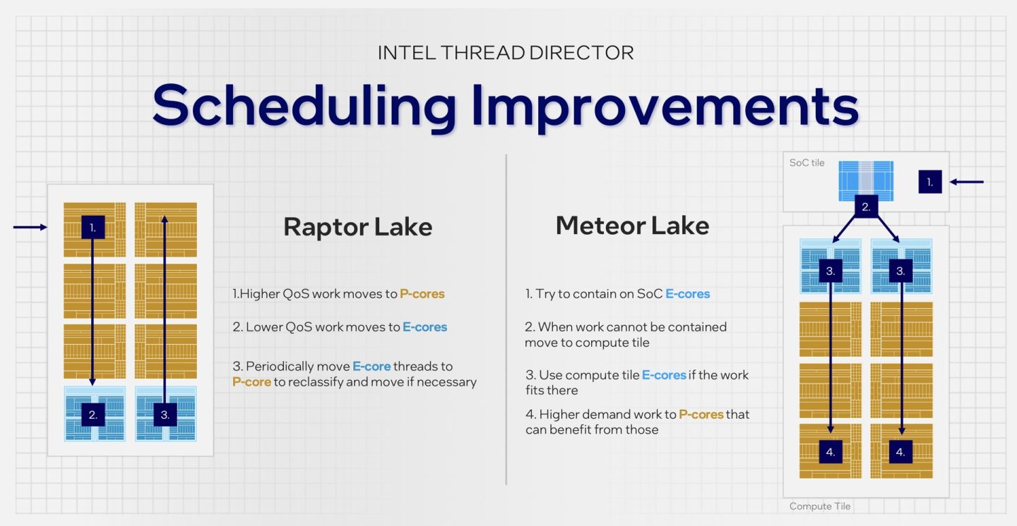
But at Intel's Innovation event this week, the company dove a little deeper into some of Meteor Lake’s advancements, describing more about how the chips would balance E-cores and P-cores and announcing its most substantial integrated GPU upgrade in years. We’ll hit some highlights below, though it’s worth watching or reading the full presentation to find out more.
Tiles for miles
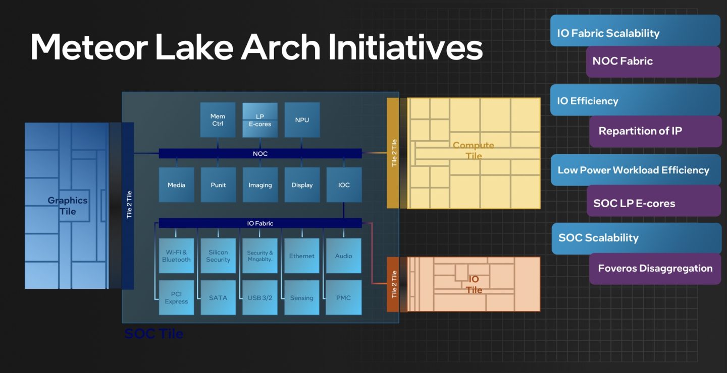
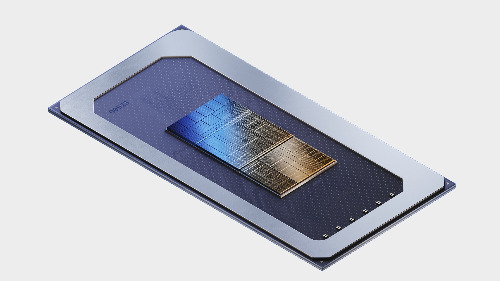
Meteor Lake will be Intel's first consumer processor to move to a chiplet-based design—instead of being one monolithic die that contains the CPU, GPU, and all the other bits and pieces needed for a modern laptop CPU, Meteor Lake is split into four "tiles" that are joined together by a fifth base tile that allows them to communicate with each other. The process of stacking the chiplets on top of the base tile is a packaging technology that Intel calls Foveros.
Here's a basic breakdown of what is in each of those four tiles:
-
- The compute tile is where most of the actual CPU is. Intel's current renderings show a chip with six high-performance P-cores based on the Redwood Cove architecture, and eight high-efficiency E-cores based on the Crestmont architecture.
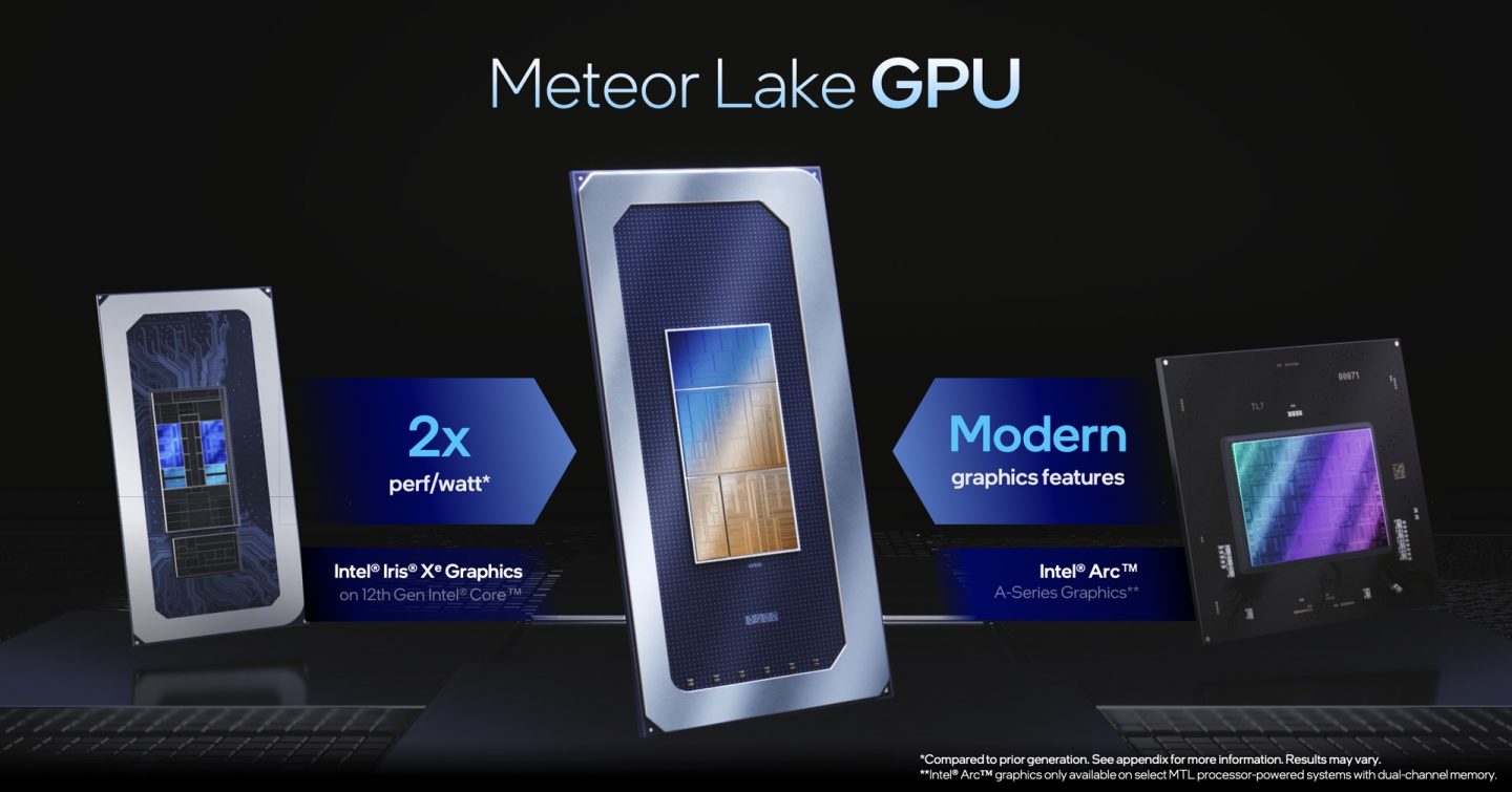
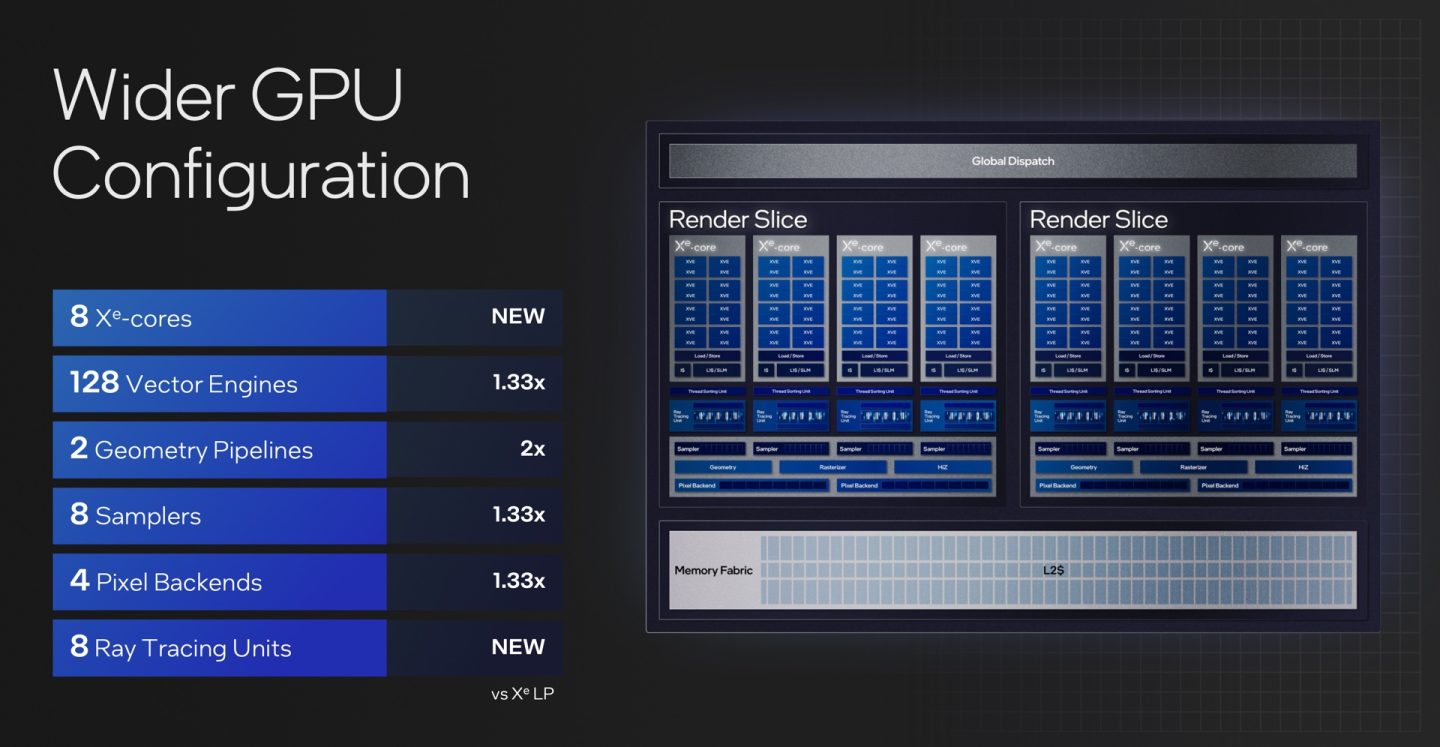
- The graphics tile is where most graphics processing happens, though a few specific functions that you'd usually find in a GPU have been moved to other tiles. Meteor Lake's integrated GPU is mostly just an integrated version of an Intel Arc dedicated GPU, complete with hardware ray-tracing acceleration.
- The IO tile handles most external connectivity, including PCI Express 5.0 lanes and Thunderbolt 4 support (Thunderbolt 5 will need to wait).
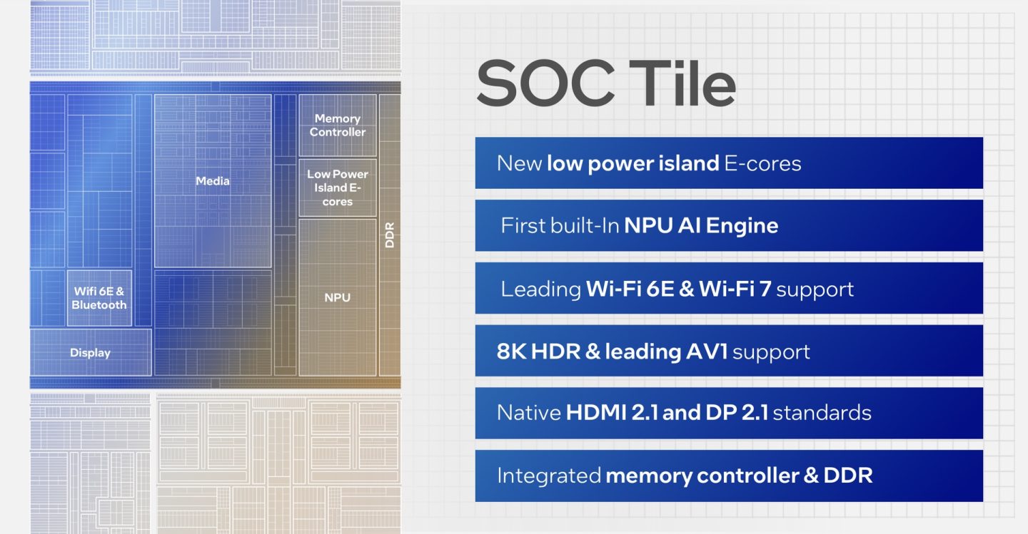
- The SoC tile is probably the most interesting of the four. It includes two additional Crestmont E-cores, the media encoding and decoding engine that would normally be located in the GPU, and the neural processing unit (NPU) used for accelerating AI and machine learning workloads. It also handles Wi-Fi and Bluetooth connectivity and connecting to external displays over HDMI 2.1 and DisplayPort 2.1.

Literally none of the manufacturers have feature-sizes that are in any way represented by the "nm" that is claimed. This change happened many years ago. In fact, it was arguably inaugurated by TSMC. You're just mad at Intel because they were late to change their marketing?
If you want to get fussy about node parity comparisons - and aren't interested in specific technologies where Intel is looking like it will actually have an advantage in the near future, like GAAFET and backside power delivery - the best metric to use would be transistor density. And by that metric, Intel 7 is at parity or better than TSMC N7 (with the real world performance to match) and by all indications Intel 4 is at parity with TSMC N4.
The hate for Intel's rebranding is just so ignorant.